LargeLanguageMind
A process-driven research journal tracing how my evolving understanding of intelligence, cognition, and machine learning emerges—from intuition, cross-domain connections, and reasoning, to formal concepts.
Neuromorphic Neurons vs “von Neumann Neurons”
Date: 2025-11-29
Last Update: 2026-08-09
Topics: neuromorphic computing, perceptron history, hardware vs software neurons, Rosenblatt’s Mark I, hardwired inference, Taalas HC1, model-specific silicon
Context: Personal reflections while reading Why Machines Learn (A. Ananthaswamy), exploring the origins of artificial neurons from McCulloch & Pitts to Rosenblatt’s Mark I, and comparing early hardware neurons with today’s software-based machine learning.
—
Abstract
This note traces how a simple question — why do we simulate neurons in software instead of building them directly in hardware? — led me from McCulloch–Pitts neurons to the forgotten history of Rosenblatt’s Mark I Perceptron, arguably the first neuromorphic computer ever built, and then forward to modern neuromorphic architectures and the possibilities they open for the next era of deep learning. By exploring this lineage, I compare three computational paradigms:
- Hardware neurons — as in the Mark I Perceptron (1958)
- Software-simulated neurons — the foundation of modern machine learning
- Neuromorphic hardware — a modern revival of Rosenblatt’s original vision (e.g., Loihi) This contrast changed how I understand the relationship between biological intelligence, digital logic, and artificial learning systems.
(2026 update: a fourth paradigm has since appeared in commercial silicon, and Section 5 covers it in detail: hardwired, model-specific inference chips such as the Taalas HC1, where the weights of an LLM are physically etched into the transistors of the die.)
1. How the Question Emerged
While reading about McCulloch & Pitts and their logical model of neurons, I stumbled onto an almost too-obvious realization: computers are built from logic gates, and so were the earliest artificial neurons. Modern deep learning, despite its scale and complexity, still boils down to differentiable arithmetic running on von Neumann hardware.
That observation triggered a simple but surprisingly deep question:
If neurons are just circuits, why do we simulate them in software instead of building them directly in hardware?
A synapse is a weighted connection.
A transistor is a controllable switch.
Both are physical, signal-processing devices.
So why not create neural networks as hardware rather than as mathematical abstractions?
Why do our “neurons” live as floating-point numbers on GPUs instead of as actual circuits?
That moment of intuition — that perhaps intelligence should be a physical architecture, not just a digital abstraction — pushed me backward into the history of Rosenblatt’s Mark I and forward into the world of modern neuromorphic computing.
—
2. Rosenblatt’s Mark I — The First Neuromorphic Machine
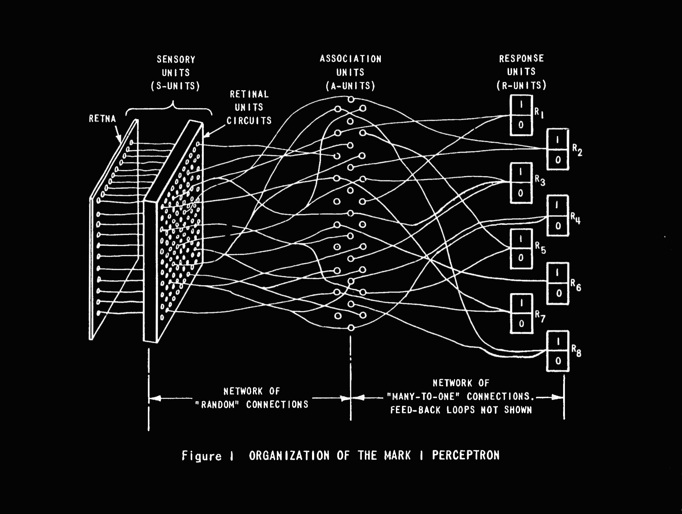 Figure: An illustration from the 1960 Perceptron Manual, representing early hardware implementations of neural networks.
What I didn’t know is that someone did try to build hardware neurons — long before deep learning existed.
In 1958, Frank Rosenblatt introduced the Mark I Perceptron, a machine built entirely from:
Figure: An illustration from the 1960 Perceptron Manual, representing early hardware implementations of neural networks.
What I didn’t know is that someone did try to build hardware neurons — long before deep learning existed.
In 1958, Frank Rosenblatt introduced the Mark I Perceptron, a machine built entirely from:
- analog circuits
- potentiometer “weights”
- physical summation units
- threshold detectors
- a photosensor array as vision input
This was not a simulation.
It was not a program.
It was a hardware neural network — arguably the first neuromorphic computer ever created.Why this matters
- It had adjustable weights (hardware learning).
- It performed classification in real-time with almost zero latency.
- The computation flowed through wires exactly like signals in a biological neuron.
In other words:
Rosenblatt tried to build a neural computer that bypassed the von Neumann architecture entirely.
His perceptron was not deep learning, but it was natively neural — structurally, electrically, conceptually.
Why it died
Criticism (especially Minsky & Papert’s XOR argument), difficulty scaling analog systems, and limited hardware technology led to the decline of perceptron research.
The tragedy is that the world abandoned Rosenblatt’s neuromorphic direction and instead embraced the general-purpose von Neumann roadmap.
Neural networks moved into software, not hardware — an understandable decision at the time, but arguably a step away from biologically inspired intelligence.
If we ever aim for truly human- or animal-like AGI, the neuromorphic path is likely to return in a much more powerful form. —3. Discovering Neuromorphic Computing (The Modern Revival)
When I searched whether anyone still builds neuron circuits today, I discovered an entire field I didn’t know existed: Neuromorphic computing — the attempt to design chips whose structure and signaling resemble biological neurons. Examples include:
- Carver Mead’s early analog VLSI neurons
- IBM TrueNorth — 1M hardware neurons
- Intel Loihi / Loihi 2 — spiking neuromorphic processors with on-chip plasticity
- BrainScaleS — analog accelerated neuron dynamics
- SpiNNaker — digital multimillion-neuron systems
This was the exact world Rosenblatt was pointing toward — a world where the neuron itself is a hardware primitive. —4. Three Worlds: Biological, Software, and Neuromorphic Neurons
Through this reading, I realized we have three different kinds of neurons:
1. Biological Neurons — analog, plastic, structurally dynamic
- Synapses strengthen or weaken (LTP/LTD)
- New synapses form or get pruned
- In limited regions, new neurons can be created (not the main learning mechanism!)
- Learning and structure are inseparable
2. Modern ML Neurons — numerical, static after training
- Represented as floating-point numbers
- Executed on von Neumann hardware
- Training is software; inference is software
- Not plastic unless explicitly programmed
3. Neuromorphic Neurons — hardware, sometimes locally plastic
- Analog or mixed-signal
- Spike-based (in contrast to CPUs/GPUs, which are synchronous clock-driven chips)
- Some support on-chip learning (like the brain’s neuroplasticity!)
- Structure fixed, but connection strengths may adapt
This helped me clarify something fundamental:Deep learning is not biologically inspired at the hardware level.
It only borrows the math of neurons, not the physics. Neuromorphic computing tries to bring hardware closer to the physics of the brain.
It is extremely energy-efficient — just like biological neural tissue — while von Neumann architecture has proven itself as a flexible and general-purpose computing model. But for achieving highly efficient, brain-like intelligence without massive data centers, a neuroplastic, spike-based hardware architecture seems like the natural future of AI. On this topic, I found two dominant viewpoints: (heard this idea from Jeffrey Shainline on the Lex Fridman podcast)- Mathematical abstraction path:
Intelligence can be represented as mathematical operations, and as long as the hardware can perform these efficiently, biologically inspired hardware structures are unnecessary. - Biological hardware path:
To unlock new paradigms of efficiency and adaptability, we must move toward hardware that is heavily inspired by the actual physical mechanisms of the brain.
- Mathematical abstraction path:
5. 2026 Update: Taalas and the HC1, or What Happens When You Etch an LLM Into Metal
Added 2026-08-09. When I wrote the original note in late 2025, I framed the question as a two-way choice: keep the math and run it on general-purpose silicon, or rebuild the substrate along biological lines. Since then a Toronto startup called Taalas has demonstrated a third answer that I did not anticipate, and it turns out to sit uncomfortably close to Rosenblatt while being about as un-biological as a chip can be. It is worth going through carefully, because it sharpens exactly what my original question was really asking.
5.1 Who Taalas is
Taalas was founded in 2023 in Toronto by Ljubisa Bajic (CEO), Lejla Bajic (COO) and Drago Ignjatovic (CTO). All three came out of Tenstorrent, which Ljubisa Bajic himself founded and led before Jim Keller took over in late 2022; before that he was a GPU and APU architect at ATI, AMD and briefly NVIDIA. Paresh Kharya, previously senior director of data center product management at NVIDIA and then AI infrastructure product management at Google Cloud, joined as VP of Products.
The company came out of stealth on 19 February 2026 with roughly 25 employees, having raised about $219 million in total ($50M in 2024, $169M in February 2026 from Quiet Capital, Fidelity and Pierre Lamond), of which only about $30 million had been spent on R&D up to the launch. On 6 August 2026, AMD announced it is acquiring Taalas, for an undisclosed sum, with the stated plan to fold the technology into its accelerator roadmap alongside Instinct GPUs.
So this is not a research curiosity. It is a working chip, and it was bought by one of the two companies that define the GPU status quo, within six months of leaving stealth.
5.2 The core idea: Hard Coded Inference
Taalas calls its architecture HC, “Hard Coded Inference.” The premise is the one I circled around in Section 1, arrived at from the opposite direction:
Instead of storing weights in memory and shuttling them to compute units, make the weights be the circuit.
Concretely, the model is burned into a mask ROM “recall fabric”: the weights are patterned directly into the metal layers of the die at manufacture. They are not loaded, not cached, not fetched. They are a permanent physical feature of the chip, exactly the way a photomask feature is permanent. That ROM fabric is paired with a smaller SRAM recall fabric which holds the things that genuinely must change at runtime: the KV cache, the context window, and LoRA-style fine-tuning adapters.
The density trick, which Bajic has deliberately not fully disclosed, is this: Taalas claims it can store a 4-bit weight and perform the multiply associated with that weight in a single transistor. Multipliers are normally the expensive part of any tensor engine, so collapsing weight storage and multiplication into one device is the whole ballgame. Bajic is explicit that this is not analog and not exotic physics: the compute is fully digital. In his words, it is “a clever trick that nobody saw because nobody went down this path,” and the design effort was “a throwback to the 1970s,” with hand transistor-level layout rather than off-the-shelf IP.
The consequence is that the memory wall, the thing that forces GPUs into HBM stacks, NVLink domains, liquid cooling and miles of copper, simply does not exist for this design. There is nothing to move.
5.3 HC1: the actual numbers
| Property | HC1 |
|---|---|
| Process | TSMC N6 (6 nm) |
| Die size | 815 mm² (near the reticle limit) |
| Transistors | ~53 billion |
| Model hardwired | Meta Llama 3.1 8B, aggressively quantized |
| On-die capacity | 8B parameters in ROM, plus SRAM for KV cache / LoRA |
| Power | ~200 to 250 W, standard air-cooled PCIe card |
| Server | 10 cards in a 2-socket x86 host, ~2.5 kW total |
| Throughput | ~15,000 to 17,000 tokens/sec per user |
| Cost | ~$0.0075 per million tokens (Taalas figures) |
For comparison on the same Llama 3.1 8B model, per Artificial Analysis and Taalas’ own internal runs: Cerebras roughly 2,000 tokens/sec/user, SambaNova around 900, Groq around 600, and an NVIDIA Blackwell B200 around 350. That is roughly a 40x to 70x gap on per-user interactivity, with about an order of magnitude better energy per token.
Two honest caveats, which the trade press flagged and which I want to keep visible: these benchmarks were run by Taalas itself, not by an independent lab, and Taalas admits its Llama 3.1 8B is quantized “aggressively,” which is a quality tradeoff of unstated size. There is a public demo chatbot, so the speed claim at least is user-checkable, but the accuracy claim is not yet independently characterized.
5.4 Why this is economically possible at all: the structured-ASIC trick
The obvious objection is: a new chip per model is insane. Taalas’ answer borrows from the structured ASICs / gate arrays of the early 2000s (Bajic explicitly names eASIC as a parallel). Everything on the die except two metal mask layers is fixed. Those two masks encode both the weights and the dataflow. Retargeting the chip to a different model therefore means a two-mask tape-out, not a full redesign.
Around that they built automation that turns model weights into RTL in roughly a week of engineering effort, with a stated two-month turnaround from an unseen model to a deployable PCIe card, developed as a “foundry optimal workflow” with TSMC. Taalas puts the cost ratio at roughly 100x cheaper to customize an HC chip than to train the model in the first place.
The hard engineering problem turned out to be verification, not design. Because nothing is programmable after tape-out, the margin for error is zero: they have to simulate the entire model, end to end, before committing metal. Design rule checking on a reticle-sized chip whose interconnect changes every spin would normally take months. Solving that was, by Bajic’s account, most of the difficulty.
A side effect I found delightful, and which speaks directly to my original point about software neurons: the software stack essentially vanished. Taalas has approximately one engineer on it, part-time. There is no kernel library, no scheduler, no graph compiler, because there is no general machine to program. The model is the machine.
5.5 Roadmap and limits
- HC2, the next generation, moves the SRAM onto a separate die, raising density to roughly 20B parameters per chip in MXFP4.
- Large models are handled by pipeline parallelism over PCIe. Because per-card latency is so low, they do not need to batch, which means bandwidth pressure between cards is low, which means plain PCIe suffices. This is a nice inversion of the usual scaling logic.
- Taalas simulated DeepSeek R1 671B across roughly 30 chips: about 12,000 tokens/sec/user at about 7.6 cents per million tokens, versus roughly 200 tokens/sec/user for a state-of-the-art GPU deployment. That still means ~30 incremental tape-outs, which Bajic concedes is “the annoying part,” though each is only two masks.
- The business model rests on one assumption, stated plainly: the customer must be willing to commit to one model for about a year. Some will not. Some, especially as model release cadence slows and users grow attached to specific model behavior, will.
TNP’s summary line for the whole category is a good one: “Model Specific Architectures.”
5.6 The connection to everything above
This is where it gets interesting for the argument in Sections 1 to 4.
First, and most importantly: the HC1 is not neuromorphic. It has no spikes. It is not analog. It is a synchronous, clocked, fully digital ASIC. It does not implement leaky integrate-and-fire dynamics, it does not do event-driven sparse signaling, and it has no on-chip learning rule. Anyone reading the headline “AI model etched into silicon” and thinking Loihi is being misled. On the biological-realism axis, the HC1 is arguably further from the brain than a GPU is, because it removed even the ability to change.
Second: it is nonetheless the strongest commercial validation to date of the half of my thesis that says “intelligence is also a substrate.” The specific claim I made was that the separation between where the weight lives and where the arithmetic happens is a historical accident of von Neumann architecture, not a property of neural computation. Taalas took that claim, applied it with total ruthlessness, and got 40x to 70x on interactivity and roughly 10x on energy per token, using a 6 nm process that is two full nodes behind what Blackwell uses. The win did not come from transistors. It came from removing the memory-compute boundary, which is exactly the neuromorphic community’s central argument, arrived at without any of the neuromorphic biology.
Third, and this is the part I did not see coming: it inverts the Mark I comparison in one crucial respect. Rosenblatt’s potentiometers were physical and adjustable; motors turned them during learning. The Mark I was hardware that could learn. The HC1 is hardware that categorically cannot: its base weights are metal. What plasticity exists is confined to the SRAM shell, LoRA adapters and KV cache, sitting on top of a frozen core.
So the axis I was implicitly treating as one dimension (“hardware neurons good, software neurons bad”) is really two:
| System | Weight is physical? | Weight can change? | Signaling |
|---|---|---|---|
| Biological neuron | yes | yes, continuously | spikes, analog |
| Mark I Perceptron (1958) | yes (potentiometer) | yes (motor-driven) | analog |
| GPU running an LLM | no (a number in HBM) | yes, trivially (rewrite memory) | clocked digital |
| Intel Loihi 2 | yes | partially, on-chip plasticity | spikes, digital event-driven |
| Taalas HC1 (2026) | yes (mask ROM) | no, frozen at fabrication | clocked digital |
Reading down the “weight can change” column, the HC1 is the most rigid system in the table, including the 1958 one. That is not a criticism of Taalas, it is precisely the trade they chose and were candid about: “we already come with this fairly serious compromise, so we wanted to make it the only one.” But it means the HC1 answers my efficiency question while making my adaptivity question strictly worse.
Fourth: my original two-path framing was incomplete. There are at least three:
- Mathematical abstraction on general hardware. Keep both the math and the flexible substrate. GPUs and TPUs. Everything is programmable, nothing is optimal.
- Mathematical abstraction frozen into substrate. Keep the math of deep learning exactly as it is, but destroy the generality of the hardware. Taalas HC1, and to a lesser extent Etched. This buys enormous efficiency and costs you the ability to change your mind.
- Biological substrate. Change both the math (spikes, local learning rules) and the physics. Loihi, BrainScaleS, SpiNNaker.
Path 2 is a genuinely new position, and it is the one that just got acquired by AMD. It is worth noting that path 2 is what the industry actually does when it becomes serious about efficiency, and it is not the biological path. That should temper the assumption I made in Section 4 that efficiency pressure would naturally push us toward the brain. Efficiency pressure pushes toward specialization. Biology is one way to specialize, but apparently not the fastest way to a product.
Fifth: the spacecraft thought experiment from my conclusion, revisited. I imagined a small assistant robot running an LLM on battery power instead of a data center. The HC1 gets you most of the way there sooner than I expected: an 8B-class model on one air-cooled 200 W PCIe card, no HBM, no liquid loop, no rack. For a probe, 200 W is still a lot, but this is an unoptimized first-generation demonstrator on N6, and the architecture’s power scales with what you compute rather than what you move. What it does not give you is the second half of what I wanted: a system that adapts on the fly, that updates its own parameters in response to a new environment. On an HC chip, the base model is as fixed as the shape of the die.
Which suggests, speculatively, that the interesting long-term architecture might be a hybrid: a large, immutable, extremely efficient hardwired core carrying the slow-changing bulk of knowledge, wrapped in a genuinely plastic layer, whether SRAM adapters as Taalas does it today or something with real on-chip learning as Loihi does it. I want to be careful not to over-sell the biological analogy here, because it is loose, but there is at least a resemblance to the way biological systems combine relatively stable large-scale structure with fast local synaptic change. I do not think Taalas is claiming this, and I would not claim it as more than an intuition.
5.7 Open questions and risks I want to track
- The performance figures are vendor-run. No independent Artificial Analysis measurement of the HC1 existed as of writing.
- The quality cost of the aggressive quantization has not been published in the form of standard benchmark deltas.
- One chip, one model, one year. If model turnover accelerates again, the entire economic argument weakens.
- The tape-out treadmill: 30 tape-outs per frontier model per year is cheap only relative to training cost, and only if two-mask spins stay cheap.
- The AMD acquisition could go either way: it could productize hardwired inference at scale, or it could quietly become a decode-side block inside a GPU roadmap, which is a much smaller idea than the one Taalas launched with.
- Taalas has filed around 14 patents under Bajic and has not published architectural papers. Almost everything technical above comes from interviews rather than peer-reviewed or ISSCC-style disclosure, so treat the mechanism claims, especially the one-transistor weight-plus-multiply, as unverified externally.
5.8 The idea I keep coming back to: a compiler that takes weights in and gives silicon out
Everything in Section 5 points at one missing piece, and I think it is the actually valuable one. Taalas built a chip. But the chip is not the interesting artifact. The interesting artifact is the toolchain that produced it.
Look again at what Bajic described: automation that goes from model weights to RTL in about a week, a two-mask customization scheme so the rest of the die never changes, a foundry-optimal workflow co-developed with TSMC, and a verification methodology that can simulate an entire model end to end because there is no post-tape-out escape hatch. Strip out the specific chip and what is left is a compiler. Its input is a .safetensors file. Its output is a set of mask layers.
5.8.1 What such a compiler actually is
Today’s stack for running a model looks like this:
model weights -> PyTorch / graph IR -> kernels (CUDA, Triton) -> fixed ISA -> fixed silicon
NVIDIA’s real moat was never only the transistors. It was CUDA: the layer that lets arbitrary math reach the metal. The stack I am describing deletes the last three boxes and replaces them with one:
model weights -> graph IR -> dataflow synthesis -> RTL -> place & route -> masks -> silicon
Call it “weights as HDL.” The model stops being a program that a chip executes and becomes a netlist specification that a chip is. The transformer’s attention pattern becomes topology. Each weight becomes a physical device. Quantization becomes a physical design constraint rather than a runtime one. Layer fusion becomes literal, wires instead of memory writes.
The layers such a compiler would need:
- Frontend. Ingest ONNX / GGUF / safetensors. Normalize architectures. Recognize repeated structure, since a 32-layer transformer is 32 near-identical blocks and that is a gift to a physical designer.
- Numerics pass. Choose per-tensor precision jointly with area and power budget. This is quantization-aware compilation, where the loss function includes square millimeters. Right now quantization is chosen by an ML engineer and area is discovered later by a hardware engineer. Those should be one optimization.
- Dataflow synthesis. Map the graph to a fixed spatial pipeline: how many physical MAC-equivalent devices, in what topology, with what pipelining depth, so that tokens flow through without ever stalling on memory.
- Partitioning. Decide what is frozen (ROM, the bulk of the weights) versus what stays programmable (SRAM, KV cache, adapters, the last few layers, embedding tables). This partition is the single most important design decision in the whole idea, and it is exactly the axis I was arguing about in Section 5.6.
- Multi-die partitioning. Cut a 671B model across N reticles, assign pipeline stages, budget the inter-die links. Taalas already does a version of this manually for their DeepSeek simulation.
- Backend. Emit RTL, run synthesis and place-and-route, emit only the differential mask layers against a fixed base die.
- Verification. The hard part. Bit-exact whole-model simulation before commit, plus formal equivalence between the original graph and the synthesized dataflow. “The compiler proves your model still says the same thing” is the feature that makes the whole thing sellable.
5.8.2 Why this is the trillion dollar shape and not the chip
Three arguments, in increasing order of how much I believe them.
The EDA argument. Synopsys and Cadence do not make chips. They make the tools that make chips, and they extract rent from essentially every silicon design on Earth with software margins and near-zero fab risk. A model-to-silicon compiler occupies exactly that position, one level of abstraction higher. If every frontier lab eventually wants its own model in silicon, the lab does not want to become a chip company. It wants to hand over a checkpoint and get back a card. Whoever owns that translation owns a toll booth on all of AI inference.
The CUDA argument. NVIDIA’s durable advantage is a compiler and an ecosystem, not a process node. Compilers are stickier than hardware because they accumulate correctness. Every model successfully taped out through such a toolchain adds patterns, calibration data and verified passes that a competitor cannot copy from a datasheet. This compounds in a way that a transistor layout does not.
The economics argument, which is the strongest one. Training a frontier model costs billions. Inference costs, integrated over the model’s service life, are now comparable or larger. Taalas’ claim is that customizing a chip to a model costs on the order of 1% of training that model. If that ratio is even roughly right, then casting a model into silicon is a rounding error on the model’s own budget and the only real question is whether the model will still be in service in a year. As release cadences lengthen and models become products with names that users are attached to, that question increasingly answers itself. The moment the answer is reliably yes, tape-out becomes a normal step in a model’s release pipeline, somewhere after RLHF and before the launch blog post.
That is the vision worth stating plainly: a chip fab in the shape of a compiler. model.compile(target="silicon"). Two months later a card arrives.
5.8.3 What is genuinely hard, and why nobody has it yet
I want to be honest about the obstacles, because the idea sounds inevitable and is not.
- Verification cost scales badly. You cannot patch metal. Every bug is a respin. Taalas already says whole-model simulation on large clusters was one of their hundred hard problems, and that was for a single 8B model. A general compiler has to be right for architectures it has never seen.
- The base die is not actually neutral. Taalas’ two-mask trick works because the rest of the die, the SRAM, the I/O, the control, is fixed and was designed for transformer-shaped workloads. A truly general compiler either needs one base die per architecture family, which erodes the economics, or a base die general enough that it starts looking like a GPU again. This tension is the central unsolved problem of the whole idea.
- You are betting against architectural change. A mask-ROM transformer is a very expensive bet that attention is permanent. State-space models, diffusion language models, or any genuinely new block resets the base die.
- Foundry coupling. This cannot be a pure software company. The backend must be co-designed with a specific process at a specific fab, which means partnership, allocation, and capacity risk. That is precisely why AMD, which has that relationship, is the natural acquirer, and why Taalas got bought within six months.
- Nobody wants to hand over their weights. The single most valuable asset a frontier lab has is the checkpoint. A compiler-as-a-service requires either on-premises deployment or a trust model that does not currently exist. This is a business-model problem masquerading as a technical one, and I suspect it is why the first movers are selling chips rather than tools.
5.8.4 Where this loops back to Rosenblatt
The reason I care about this beyond the business framing: a model-to-silicon compiler is the general machine for building Mark I Perceptrons.
Rosenblatt hand-built one network into hardware and it took a room, a photosensor array, and motors to turn the potentiometers. The reason nobody repeated the exercise at scale was not that hardware neurons were a bad idea. It was that translating a trained network into a physical artifact was a bespoke, manual, un-repeatable act of engineering. That is exactly the problem a compiler exists to solve.
If such a toolchain matures, then “should this network be software or hardware?”, the question I started this whole note with in Section 1, stops being a philosophical choice about the nature of intelligence and becomes a build flag. You would train in software, because gradients need flexibility, and deploy in silicon, because inference does not. The frozen half of the brain gets etched. The plastic half stays in SRAM.
And then the remaining question, the one I do not think a compiler solves and the one Section 5.6 keeps circling, is whether the plastic half can ever be made large enough to matter. A compiler that only emits frozen weights gives us extremely efficient fossils. The version of this idea I would actually want to build is the one where the compiler’s partitioning pass is a first-class knob: you tell it how much of the model must remain able to change, and it decides what to cast in metal and what to leave alive.
That, I think, is the interesting startup. Not “we hardwire LLMs.” Rather: “you give us a model and a plasticity budget, and we give you the physics.”
Conclusion
I can imagine a neuromorphic chip running an LLM-like AI inside a small assistant robot on a spacecraft, powered only by compact batteries — not massive data-center servers trying to predict the next word on general-purpose GPUs. I imagine a system with true hardware-based artificial plasticity, able to adapt and update its own parameters on the fly, instead of the static, frozen-weight models we use today that rely on constantly shifting external inputs to simulate memory.
Biological intelligence is not a piece of software — it is a physical, adaptive, constantly changing neural substrate.
Rosenblatt understood this, which is why the Mark I Perceptron was a machine built from neurons as hardware, not neurons as equations.
The world abandoned that direction and pursued the von Neumann model, where neural networks became code executing on general-purpose processors. It was a practical choice, but one that pushed AI away from the physics of the brain.
Neuromorphic computing attempts to reconnect these two worlds.
Its spike-driven, massively parallel, event-based design mirrors the principles that give the biological brain its astonishing efficiency.
For tasks requiring continual learning, real-time adaptation, or extremely low power consumption, neuromorphic hardware offers capabilities that digital deep learning struggles to match.
Whether AGI emerges from mathematical abstraction running on digital hardware, or from hardware designed to emulate biological principles, remains an open question.
But it is increasingly clear that the long-term future of AI — especially if we seek brain-like efficiency — may require a return to Rosenblatt’s original insight:
Intelligence is not only an algorithm; it is also a substrate.
Addendum, August 2026. Taalas is the clearest evidence yet for the second half of that sentence and the clearest counter-evidence to how I got there. The industry did move the model into the substrate, it did get a large efficiency win, and it did so by ignoring biology entirely. What it gave up was adaptivity, which is the one property the brain never gives up. If I had to restate the closing line now, it would be: intelligence is an algorithm, a substrate, and the ability to keep changing both. Nobody has all three yet. Taalas has the substrate. Loihi has the change. GPUs have the algorithm, and the electricity bill to prove it.
Disclaimer
This note reflects only my current understanding of neuromorphic computing, hardware, and machine learning at the time of writing.
It is not meant to be a formal academic text, and some explanations are intentionally simplified.
I have tried to fact-check the main claims and avoid obvious misunderstandings, but there may still be gaps or inaccuracies.
The purpose of this document is to track my own learning process, not to present a final or authoritative view on the topic.
Specifically for Section 5: Taalas has not published peer-reviewed papers on its architecture, and the performance numbers cited are the company’s own. Read them as claims, not as measurements.
—
Further Material
- Why Machines Learn: The Elegant Math Behind Modern AI — Anil Ananthaswamy
- Computerphile: “Neuromorphic Computing”
- Fraunhofer IIS: Neuromorphic Computing Overview
- Architecture All Access: “Neuromorphic Computing Part 1 & 2”
Sources for Section 5
- Timothy Prickett Morgan, Taalas Etches AI Models Onto Transistors To Rocket Boost Inference, The Next Platform, 19 Feb 2026
- Sally Ward-Foxton, Taalas Specializes to Extremes for Extraordinary Token Speed, EE Times, 19 Feb 2026
- Timothy Prickett Morgan, With Taalas, AMD Can Bake AI Inference Directly Into Its Chippery, The Next Platform, 7 Aug 2026
- AMD buys Taalas, startup that hardwires AI models into its silicon, CNBC, 6 Aug 2026
- AI chip startup Taalas raises $169m, unveils HC1 processor optimized for Llama 3.1 8B, Data Center Dynamics
- AI inference cast in silicon: Taalas announces HC1 chip, heise online
- Taalas patent filings under Bajic, Google Patents
- Taalas HC1 public demo: chatjimmy.ai
Author: TheMindDeveloper GitHub: https://github.com/theMindDeveloper Email: theminddevlab@gmail.com